Key learning points
- PCBs are manufactured using CNC machining or chemical etching
- PCB design involves placing components, creating tracks and pads, and using design software
- PCB amendment involves updating components, modifying tracks, and repositioning pads
- PCBs are used for space-saving, reliable connections, ease of repair, and professional appearance
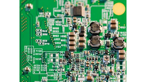
Manufacturing printed circuit boards (PCBs)
There are two main ways to manufacture printed circuit boards (PCBs):
- CNC machining
- Chemical etching
Find out How to produce a PCB safely
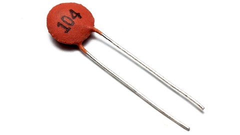
Why use PCBs?
- space-saving compared to just using components soldered using loose wires
- easier to repair - just swap components
- more reliable connections
- professional appearance
How to design a PCB from a circuit diagram
The two diagrams above are of the same circuit for a simple night light.
How it works: when darkness falls on the light dependant resistor (LDR), its resistance increases causing a higher voltage out from the potential divider. This now allows the base leg of the NPN transistor to switch on, allowing current to flow from the collector to the emitter legs, activating the LED.
When designing a PCB from a circuit diagram, there are key considerations to make:
- Component placement:
- identify components: start by identifying all the components in the circuit diagram.
- positioning: place the components on the PCB layout, ensuring they are positioned logically and efficiently. Keep related components close to each other to minimize track lengths.
- orientation: ensure components are oriented correctly, with their pins matching the connections in the circuit diagram.
- Creating tracks and pads:
- Tracks: draw tracks (the conductive paths) to connect the components as per the circuit diagram. Ensure the tracks are wide enough to handle the required current.
- Pads: place pads (the areas where components are soldered) at the ends of the tracks. Ensure pads are appropriately sized for the component wires.
- Design software: use PCB design software to create the layout. PCB design software helps in accurately placing components, tracks, and pads.
When amending a PCB design, consider the following:
- Reflecting changes:
- Update components: if the circuit diagram changes, update the components on the PCB layout accordingly.
- Modify tracks: adjust the tracks to reflect the new connections. Ensure there are no short circuits or unconnected paths.
- Reposition pads: move pads if necessary to accommodate new component positions or changes in track layout.
- Improving designs:
- Optimize layout: rearrange components and tracks to improve the efficiency and performance of the PCB.
- Error correction: Check for and correct any errors in the initial design, such as overlapping tracks or incorrect pad sizes.
- Design review: regularly review the PCB design to ensure it meets the required specifications and functions correctly.
Example
Below is a circuit diagram for a greenhouse fan. When the greenhouse becomes too hot (above 27 degrees Celsius), a motor fan will switch on to cool the greenhouse down.
A pupil is manufacturing a PCB based on the greenhouse fan circuit diagram. The incomplete PCB is shown below. Add the following components:
- 10k resistor
- Transistor
- Motor
- Diode
How it works:
- the microcontroller has been programmed to check the analogue signal for when the thermistor goes above 27 degrees Celsius.
- when it goes above 27 degrees Celsius, it makes the output go high, switching on the base leg of the NPN transistor. This will allow current to flow from the collector and emitter pins, switching on the motor fan.
- the diode is placed across the motor fan to stop back EMF.
A simple flowchart for this PCB is shown below:
Test yourself
More on Electronic and microelectronic control systems
Find out more by working through a topic
- count3 of 12
- count5 of 12

- count6 of 12